I used to follow a smartphone reviewer on Chinese TikTok. He once said there’s no way chip technology could go smaller than 3 nm. Well, you know what? IBM just gave him not one, but two slaps across the face.
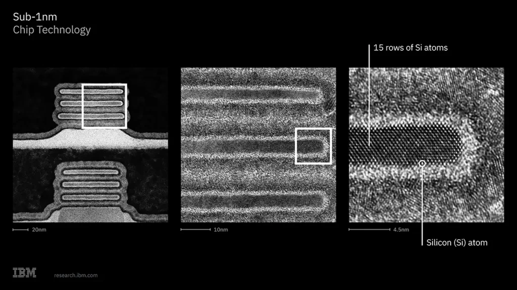
The computing giant has unveiled the world’s first sub-1 nm chip technology. Not 2 nm. Not 1 nm. We’re talking 0.7 nm, or 7 angstroms if you want to sound smarter than everyone else at the dinner table. Better yet, IBM believes it can turn this into a real product in the next five years.
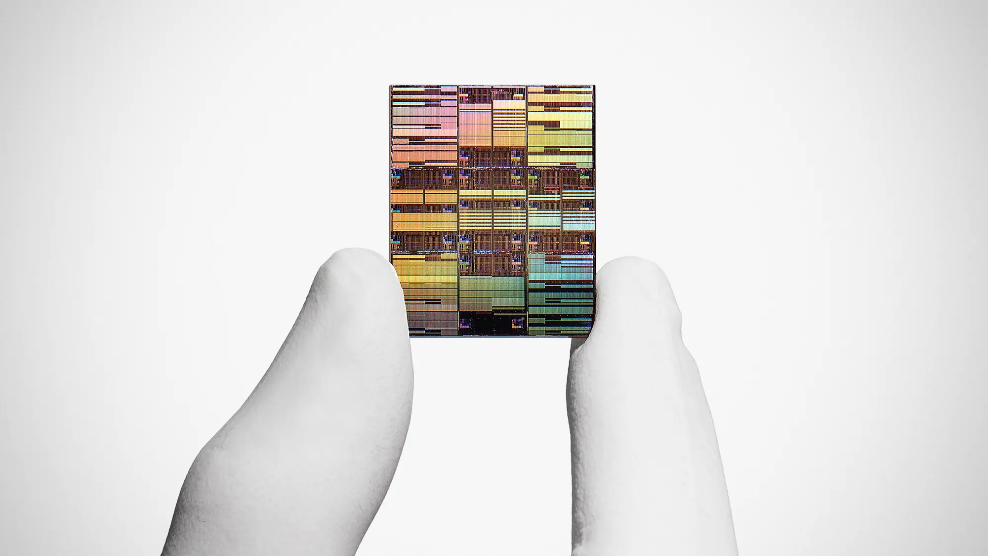
Shrinking chips has become increasingly difficult over the years. Engineers have been squeezing more and more transistors into the same space, and many believed the industry was approaching the physical limits of silicon. IBM’s answer? Stop thinking in two dimensions. Instead of simply shrinking transistors, it stacks them vertically using a new three-dimensional design called Nanostack, allowing nearly 100 billion transistors to fit onto a chip roughly the size of a fingernail.
According to IBM, the new design could deliver up to 50 percent more performance or 70 percent greater energy efficiency than its 2 nm technology. That’s good news for everything from AI servers and cloud computing to smartphones, laptops, and just about every electronic device that depends on faster, cooler, and more efficient chips.
IBM also believes the new architecture can keep chip technology moving forward for at least another decade. So the next time someone confidently tells you chips can’t get any smaller, you know what to tell them. Maybe don’t mention the two slaps, though.
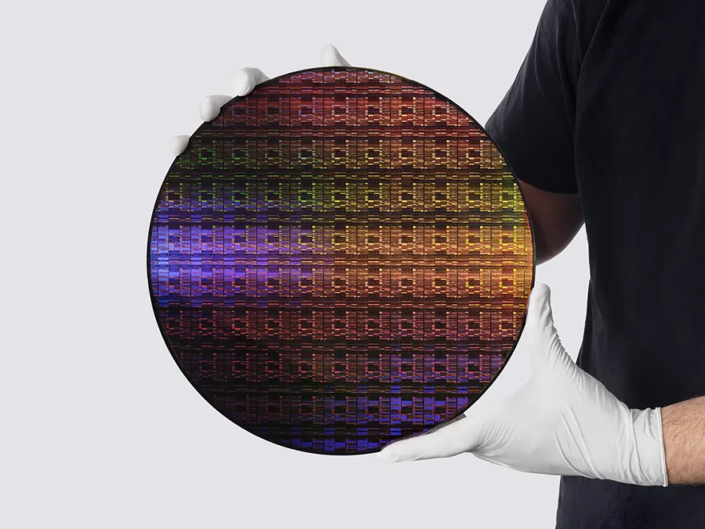
Images: IBM.